Joint Lab with companies
In the framework of the PNRR MUSA Project, three industry-university Joint Labs have been activated to develop highly specialized research and, in perspective, open up to external collaborations:
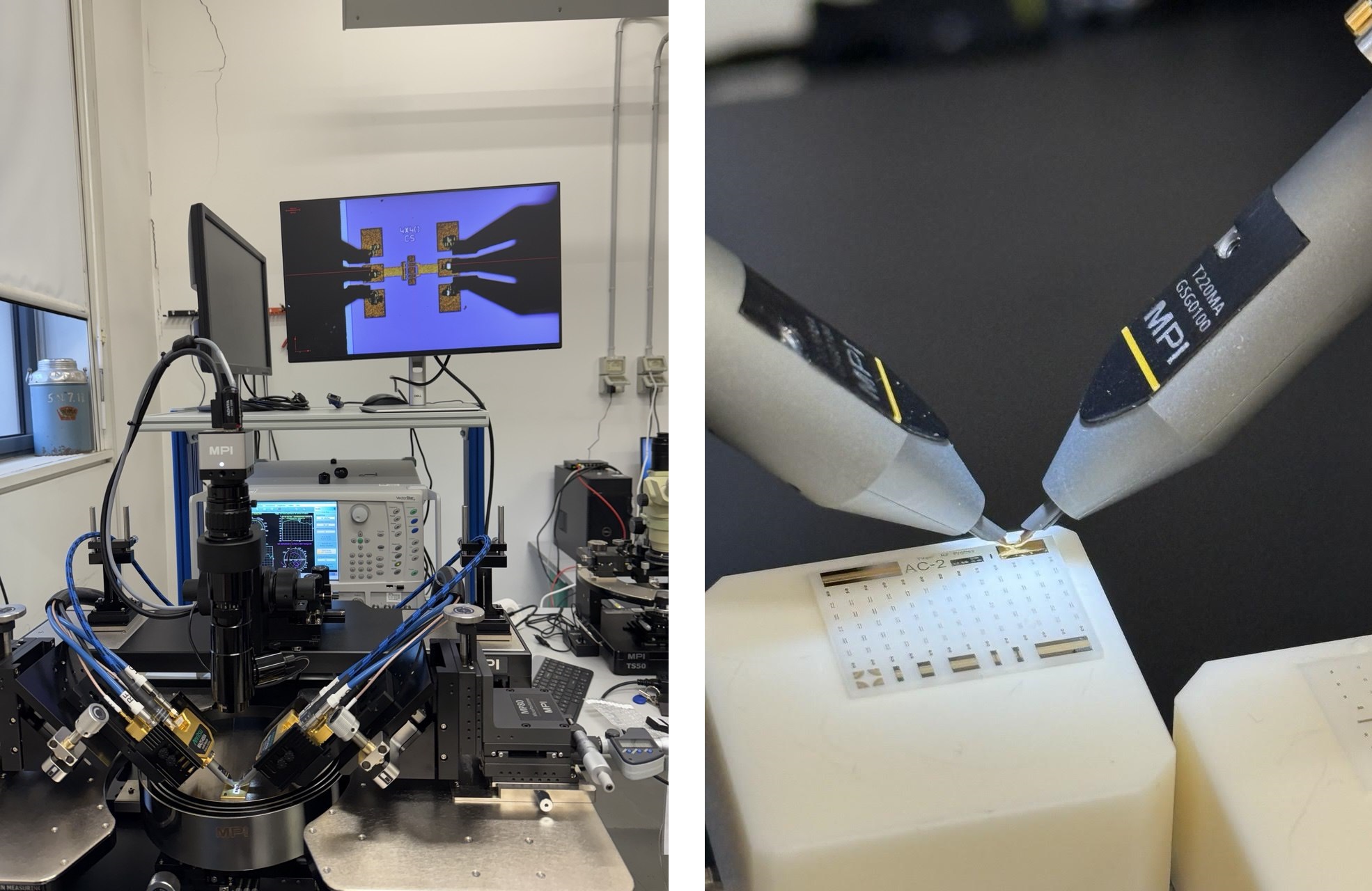
- The “mm-Wave Electronics Laboratory” (WELab), in collaboration with Huawei, is dedicated to the development of characterization techniques suitable for measuring electronic devices at sub-THz frequencies (> 100 GHz) and accurate transistor modeling for the design of integrated circuits operating at sub-THz frequencies. The Laboratory is equipped with a state-of-the-art 2-port vector network analyzer (VNA) for broadband characterization from 9 kHz to 220 GHz. In addition, general-purpose tools for characterizing electronic devices and IC prototypes are available, including: semiconductor parameter analyzer, MPI manual probing station for on-wafer characterization, digital oscilloscope (1 GHz bandwidth), arbitrary function generator (AFG, 350 MHz), multimeter, DC power supplies, and soldering station.
-
The “Automatic Test Laboratory” (ATLab), in collaboration with Infineon, is dedicated to the development of automatic test solutions for industrial power devices, such as gate drivers, and to the research and evaluation of methodologies for modeling and simulating test setups. The laboratory is equipped with a Teradyne ETS-88, an automatic test system widely used in industry and characterized by high versatility and efficiency, and the semi-automatic Cascade TESLA200 prober, used to interface the ATE with industrial silicon wafers. In addition, the ATLab is equipped with additional specific instrumentation for electronic device testing and test hardware development, including: a device for the thermal control of the DUT via mechanical contact, a 6-channel analog oscilloscope (1 GHz bandwidth), a fully equipped soldering station and generic laboratory instrumentation.
-
The MIB-TASI Joint Laboratory conducts research activities focused on the design, characterization and testing of analog and digital devices intended for radiation-hardened aerospace applications. These include components such as microprocessors, gravitational accelerometers, oscillators and memory units. The MIB-TASI JLAB provides remote access to servers for the design of silicon integrated circuits using advanced nanoscale technologies, including 28 nm CMOS and 16 nm and 7 nm CMOS FinFET nodes. It is also equipped with a rich instrumentation both automatic via the Keysight PXI modular system and manual for the characterization of devices up to hundreds of MHz. The Joint Laboratory is also a think-tank where new ideas on scientific payloads, advanced sensing and AI-based data analysis algorithms are developed.
